Tips for Laying out a Schematic in Eagle
|
|
Constructing a Schematic in Eagle
Breadboards are great for prototyping circuits but eventually we need a more permanent and reliable solution for creating circuits. That is when we create custom PCB (Printed Circuit Boards). The following section outlines how to create a circuit schematic in Eagle (which you can download from the Software page).
Eagle is a program from www.cadsoft.de that enables users to draw the circuit diagram for anelectronic circuit and then layout the printed circuit board. This is a very quick start tutorial, where you will be led step by step through creating a PCB for a darkness detector.
Eagle is a program from www.cadsoft.de that enables users to draw the circuit diagram for anelectronic circuit and then layout the printed circuit board. This is a very quick start tutorial, where you will be led step by step through creating a PCB for a darkness detector.
|
1. After installing Eagle open it up and you will see the control panel (figure 1)
|
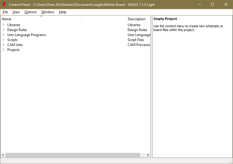
Figure 1
|
|
2. On the menu go to FILE then NEW then SCHEMATIC
3. You will see the schematic editor open (figure 2) |
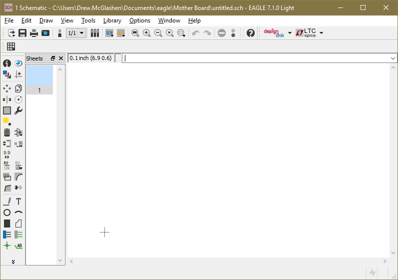
Figure 2
|
|
4. Save your new schematic
5. Within the Eagle folder create a folder for the name of this project e.g. DarkDetector 6. Save the schematic inside the folder you just created e.g. 'DarkDetector_v0.sch' within the DarkDetector folder. 7. If you go back to the control panel you should see a folder with the schematic file you created inside it e.g the 'DarkDetector' folder has the 'DarkDetector_v0.sch' file inside it (figure 3) |
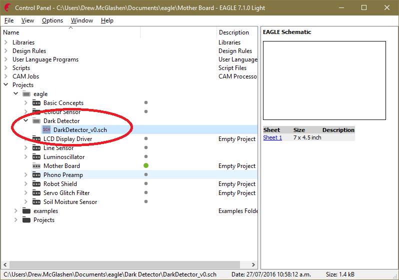
Figure 3
|
|
The first part of the process in creating a PCB is drawing the schematic. Parts will be added from libraries and joined together using ‘nets’ to make the circuit.
As you point to the tools in the TOOLBOX their names will appear in a popup and also their description will appear in the status bar at the bottom of the window 8. Find the following tools
9. Download the waimea Eagle library from the software page here and save it in your Eagle library directory (by default: 'C:\EAGLE-7.1.0\lbr') 10. From the menu select 'Library-Use...', navigate to where you saved the waimea library file and open it (figure 5) 11. From your schematic Click the ADD button in the toolbox. A new window will open (it may take a while). Find the 'waimea_v1' library, open it by double clicking on it or by clicking the > sign. Add the components you need to complete your schematic. For example: Open the R-EU_ section (Resistor-European). Here you will find the 0204/7 resistor. Select it and then click OK. Add 2 more resistors of the same type. 12. Continue adding parts until you have added everything your schematic requires. You can add more later as well as copy and paste components you have already added. For my example I will add all of the following parts (figure 6):
|
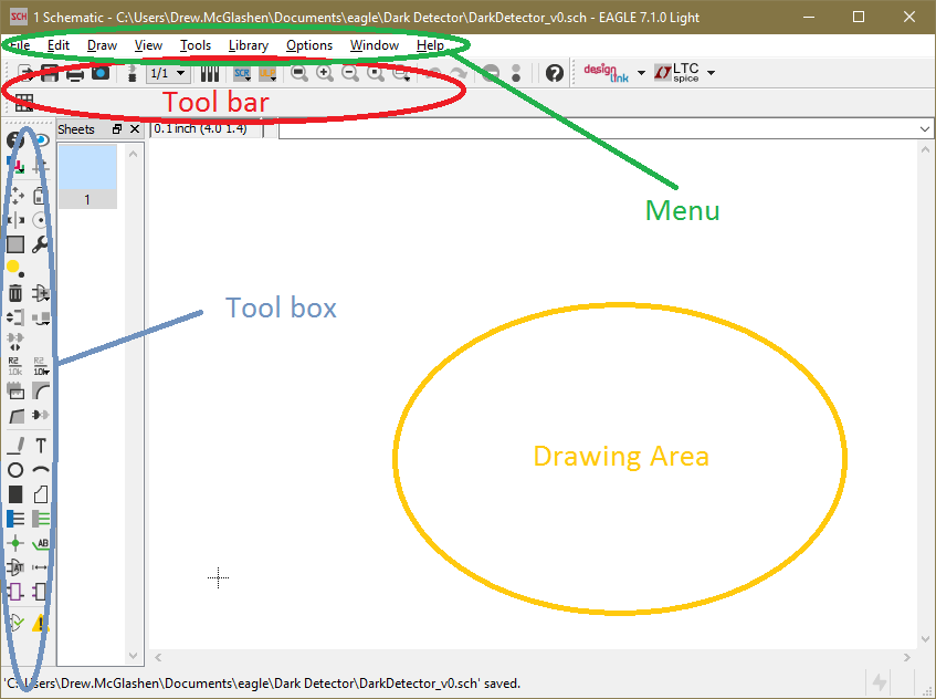
Figure 4
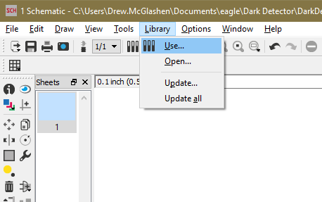
Figure 5
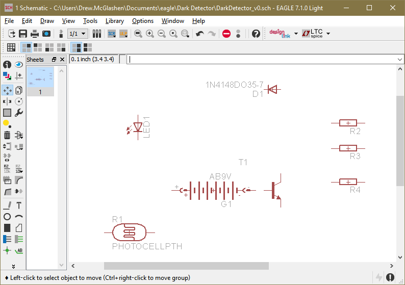
Figure 6
|
|
13. Now use the 'Move an object' tool in the TOOLBOX to move the components where you want them. Left click to select, when selected you can right-click to rotate and then left click again to place. (figure 7)
|
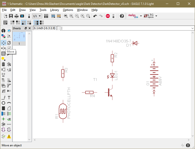
Figure 7
|
|
14. Now you can use the 'Net' tool to join together the pins of your components (figure 8). These form the electrical connections that makeup the circuit.
A green dot should appear when you join nets together. If it doesn't it might mean the nets are passing over one another but are not actually connected. Each net has a unique name. Find the info button in the toolbox and check the names and details of the components and nets. When you want to connect a new net to an existing net, Eagle may prompt you as to which name to give the combined net. If one of the nets has a proper name i.e. VCC, V+,V-, ground... use that name, otherwise choose the net with the smallest number. 15. There is an easy way to check each pin of your components is connected to a net. Select the move tool and move a component around a little. If the nets remain attached to the components then they are correctly attached (figure 9). |
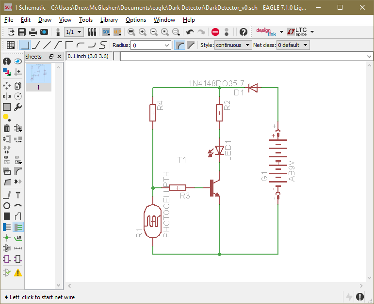
Figure 8
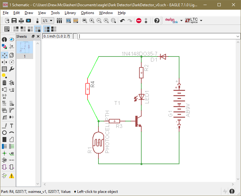
Figure 9
|
|
16. The ERC button causes Eagle to test the schematic for electrical errors. Errors such as pins overlapping, and components unconnected are very common.
The ERC gives a position on the circuit as to where the error is; often zooming in on that point and moving components around will help identify the error. You must correct all errors before going on. |
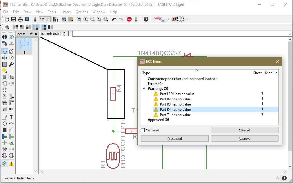
Figure 10
|
Tips for Laying Out PCB in Eagle
|
|
|
1. Now you have a schematic you can create yourself a PCB. The board editor is opened using a button in the toolbar, find this button and answer yes to the question about creating the board (figure 11).
|
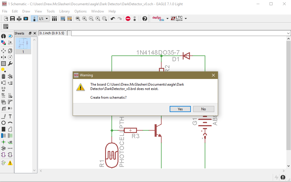
Figure 11
|
|
2. The new window has a pile of parts and an area upon which to place them (figure 12).
WARNING: once you have started to create a board always have both the board and schematic open at the same time, never work on one without the other open or you will get horrible errors which will require you to delete the .brd file and restart the board from scratch. Laying out PCB is hard. It is hurts your brain hard. It is so hard computers can't do it well. Thanks to evolution our brains are actually quite good at it, finding patterns, seeing alternative routes etc. It is still hard though. Anyway here are some tips that will help you have some more success with layout out PCB: |
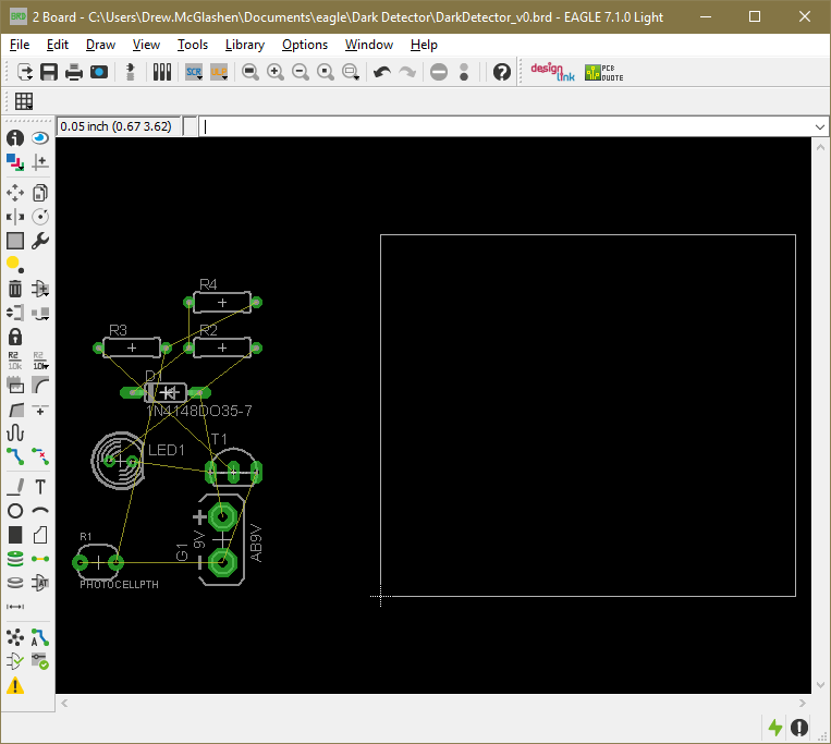
Figure 12
|
|
To help you layout your PCB the nets from the schematic have become connections called airwires, these wires will shortly become tracks of your PCB. These connections can look very messy at times and at this stage it is called a RATSNEST.
3. Move the components into the highlighted area. In the demo version you cannot place parts outside this area. Keep the components in the lower left corner near the origin (cross). Reduce the size of the highlighted area you are using for the components. Then zoom to fit (figure 13). |
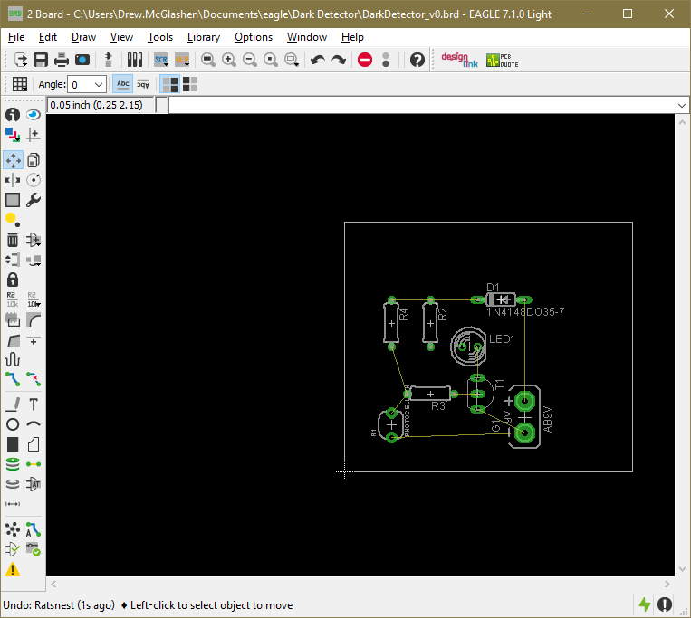
Figure 13
|
|
4. Progressively arrange the components so that there is the minimum number of crossovers. As you place components press the Ratsnest button often to reorganize the Airwires (figure 14).
Good PCB design is more about placement of components than routing, so spending most of your time (80%) doing this step is crucial to success. You want to make track lengths as short as possible |
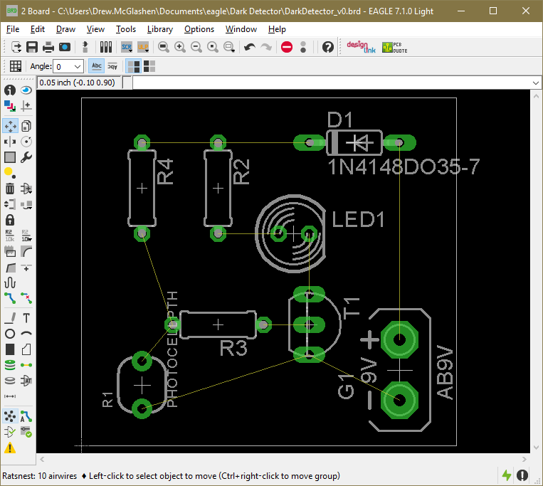
Figure 14
|
|
Now is the time to replace the airwires with actual PCBtracks. Tracks need to connect all the correct parts of thecircuit together without connecting together other parts. This means that tracks cannot go over the top of one another, nor can they go through the middle of
components! 5. Go to the Toolbox, Select the ROUTE button. 6 . On the Toolbar make sure the Bottom layer is selected (blue) and that the track width is 0.04. Left click on a component. Note that around your circuit all of the pads on the same net will be highlighted. Route the track by moving the mouse and left clicking on corner points for your track as you go (figure 15). YOU ONLY WANT TO CONNECT THE PADS ON THE SAME NET, DON'T CONNECT ANY OTHERS OR YOUR CIRCUIT WILL NOT WORK. 7. Click on a pad to finish laying down the track. Track layout Rules
Ripping up a track is removing the track you have laid down and putting the airwire back in place. This will be necessary as you go to solve problems where it is not possible to route the tracks. You may even want to rip up all the tracks and move components around as you go. |
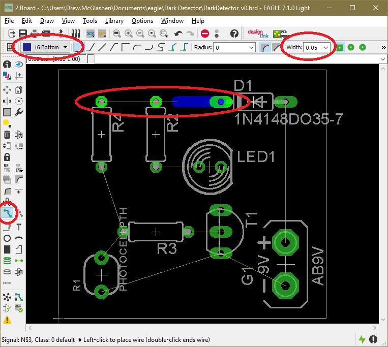
Figure 15
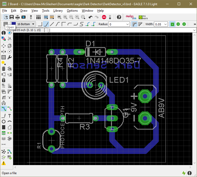
Figure 16
|
|
Finally it is time to print your PCB.
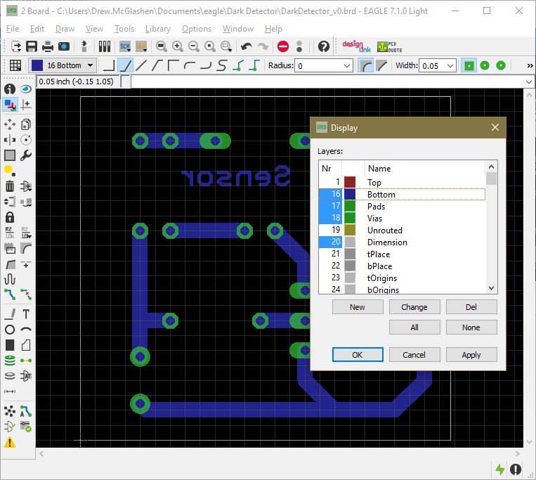
8. Firstly you need to switch off all of the layers except '16 Bottom', '17 Pads', '18 Vias' and '20 Dimensions'. You do this using the 'Show/hide/edit layers' tool (figure 17). |
|
|
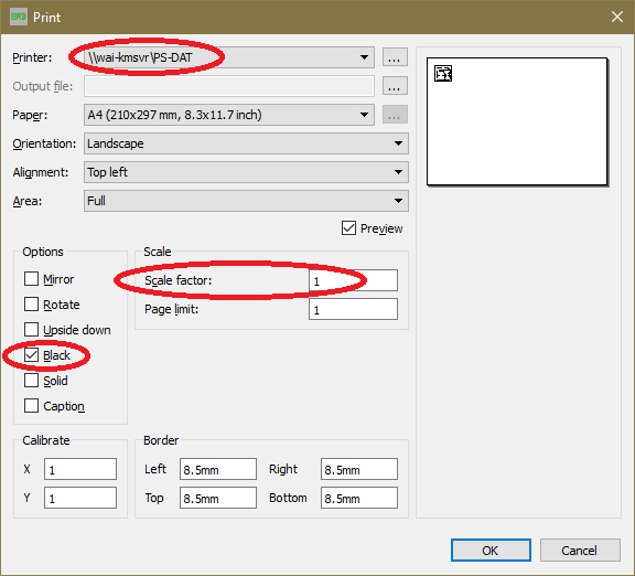
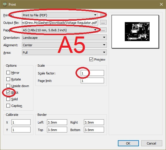
9. Then hit Ctrl+P to open the printing dialog. Make sure you set the 'Scale Factor' to 1 and check 'Black' in the options list.
If you are printing from your computer set the paper size to A5 and select 'Print to File (PDF)' as your printer, save the file and then print the file from this site If you are printing from a school computer you can print to 'PS-DAT' |
|
Creating a PCB
|
|
This video covers most of the techniques that we will use but with a few differences. We will transfer the the printed PCB layout onto a yellow transfer film before using the laminator to put it onto the copper PCB.
We use rotary tool drill presses for for drilling the holes in the PCB. It is important to hold your work down firmly when using these and make sure the bit is fully retracted before moving the PCB. If you do break a bit please let me know so I can give you another one and order some more. Cheers. |

